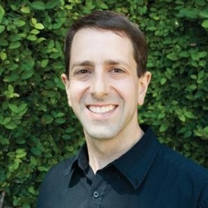
J. Alex Chediak
- Courses4
- Reviews15
- School: California Baptist University
- Campus:
- Department: Physics
- Email address: Join to see
- Phone: Join to see
-
Location:
8432 Magnolia Avenue
Riverside, CA - 92504 - Dates at California Baptist University: February 2009 - February 2019
- Office Hours: Join to see
Biography
California Baptist University - Physics
Resume
1999
English
Spanish
Doctor of Philosophy (Ph.D.)
Materials Science & Engineering
University of California
Berkeley
1996
IBM
Northwestern College
Cypress
AlexChediak.com
UC Berkeley
California Baptist University
Burlington
Vermont Area and East Fishkill
NY
Held several positions: LPCVD Hot Process Engineer
Fabless Semiconductor Program Manager and Product Integrator
Photolithography Development Engineer
CMOS Process Integration Engineer.
Process Development Engineer
IBM
Riverside
CA
My core objective is to raise the stature
quality
and effectiveness of our academic personnel
particularly our 320+ full-time
tenure-track faculty. I serve as a liaison between Senior Administration (the Provost Office and the Vice-President for Online and Professional Studies) and the Faculty
provide leadership in the professional development of the faculty
act as an advocate for the faculty
and work collaboratively with members of the Executive Council on matters such as faculty motivation
compensation
and overall effectiveness (in teaching
scholarship
and service). I serve on the Presidential Advisory Committee
the Provost Council
and as Chair of the Faculty Appeals Committee. I lead the twice-monthly Faculty Senate meetings with 40 faculty members elected from among over 320 full-time faculty. I strive to be winsome and collegial in my interactions with faculty
staff
and Administrators
believing firmly in the principles of shared governance
the golden rule (Luke 6:31)
and respect for authority.
Faculty Senate President
California Baptist University
Saint Paul
Minnesota
Taught algebra-based and calculus-based physics classes (mechanics
electricity
magnetism
optics)
as well as engineering electives. Advised 3/2 Dual-Degree engineering students
developed curriculum for engineering courses
and recruited for the Dual Degree engineering program. Wrote several vision-casting white papers for the Vice President. I wrote an article on the opportunities within the field of engineering for the Fall 2006 alumni newsletter (to increase awareness among alumni
donors and prospective students of the college’s initiatives). Initiated a scholarship fund to financially support engineering students. Served on the Eagle Scholars Program Committee (the equivalent of Northwestern College’s Honors Program).
Assistant Professor
Northwestern College
Riverside
CA (or wherever I am needed)
As the author of Beating the College Debt Trap (Zondervan
2015)
Preparing Your Teens for College (Tyndale House
2014) and Thriving at College (Tyndale House
2011)
it's my pleasure to speak for churches
youth groups
and conferences on issues related to my writing. For more about my books
articles
and other writing
see www.alexchediak.com.
Writer
Speaker
AlexChediak.com
Teach physics courses and discharge various committee work. I'm interested in learning more about what helps students learn
retain what they've learned
and experience long-term academic and professional success.
California Baptist University
Associate Professor of Physics and Engineering
Teach physics courses and discharge various committee work. I'm interested in learning more about what helps students learn
retain what they've learned
and experience long-term academic and professional success.
California Baptist University
Physics Faculty Representative
Serve as the primary liaison for all physics issues at the university. Interact in this capacity with the Associate Dean of Natural and Mathematical Sciences
the Dean and Associate Deans in the College of Engineering
the Dean and Associate Deans in the College of Architecture
Visual Arts
and Design (CAVAD)
and key members of the College of Health Sciences. Schedule physics classes and lab sections (about 75 units/semester). Manage the utilization
support
and development of two large
teaching & laboratory spaces for holding physics courses with laboratory components. These labs each contain about $200
000 worth of equipment and supplies. Oversee and recruit physics adjuncts and lecturers. Advise our growing cadre of physics minors. Lead discussions of curricular initiatives in the area of physics. Perform long-term planning with regard to the need for physics faculty and instructional space. \n\nIn my first academic year in this role
I recruited two new adjuncts
raised the number of course offerings in physics by 50%
and filled all physics courses & lab sections to ~90-100% capacity—all without the addition of any tenure-track faculty. This dramatically lowered per-pupil instructional costs. I secured new computers for both physics labs. I secured an upgrade to the instructional technology in our two dedicated physics classroom spaces.
California Baptist University
Cypress
Bloomington
MN
I was responsible for 365 nm and 248 nm lithography modules for a non-volatile memory program. I was also involved in a company-wide collaboration for advanced photolithography process development (193 nm) with U.C. Berkeley (FLCC). I was trained on high-NA
193-nm ASML scanners for a portion of this work. I later assisted in the development of a CMOS-based image sensor at the 0.18um technology node. My responsibilities included process integration for both front end of the line and back end of the line (aluminum) process steps. I also interfaced with characterization and test engineers in order to improve device performance to meet customer expectations.
Development Engineer
1992
Bachelor of Science (B.S.)
Ceramic Engineering
Tennis Team
Cross-Country Team
Student Judicial Board
Alfred University
940
A bullet-proof fabric containing a first layer of high-strength fabric
a first layer of ceramic material below the first layer of high-strength fabric
and a second layer of high-strength fabric disposed below the first layer of ceramic material. The first layer ceramic material contains a multiplicity of ceramic structures
each of which has a first orifice extending through it
and a means for fastening the ceramic structure disposed within the orifice.
us
Ceramic bullet-proof fabric
Daniel Edson
772
A method and structure for a programmable circuit that includes a magnetic device having a reluctance which is alterable. The magnetic device can be programmed into one of three magnetic field orentations or states. Conventional VLSI fabrication steps are used for compatability with low-k dielectric Back-End-Of-Line (BEOL) processing.
us
Re-settable tristate programmable device
Richard Williams
Wilbur D. Pricer
William T. Motsiff
Kurt Kimmel
647
A method of forming a dual damascene pattern in a dielectric
includes etching a pattern of lines minus vias overlapping the lines to a line depth
leaving the dielectric unetched at the via locations; while the vias are etched in a separate step
starting from the top surface of the dielectric and continuing to a via depth greater than the line depth.
us
Via masked line first dual damascene
Andrew Lu
455
The present invention relates to a functionally integrated microanalytical system for performing fluorescence spectroscopy. A source of fluorescence-exciting radiation
typically a LED
is integrated onto a substrate along with a photodetector and
in some embodiments
an optical filter. A pixel-to-point laser lift-off process is used to effect this component integration. For those cases in which a filter is required
a thin film bandgap filter is typically used
such as CdS or CdS.sub.xSe.sub.1-x (0
photodetector and (optionally) filter. This configuration of components allows the microchannel and sample to be readily removed and replaced
facilitating rapid analysis of multiple samples. Multiple LEDS
detectors and filters (if present) can also be integrated onto the same substrate
permitting multiple wavelength analysis of the sample to be performed concurrently.
us
Integrated
fluorescence-detecting microanalytical system
376
A method of forming conductive contacts to drain and source regions of a semiconductor device such as a field effect transistor (FET). A gate structure is formed over a portion of a semiconductor substrate
wherein the gate structure includes: a gate dielectric on a surface of the semiconductor substrate
a conductive gate aligned on the gate dielectric
a silicide layer aligned on the conductive gate
and a silicon nitride cap aligned on the silicide layer. Insulative spacers are formed on sidewalls of the gate structure
and the insulative spacers contact the semiconductor substrate. A drain region and a source region are formed within the semiconductor substrate
wherein a channel region is disposed between the drain region and the source region
and wherein the gate structure is over the channel region. After an insulative region containing a photosensitive material
such as boro-phoso-silicate glass
is formed over the gate structure and the semiconductor substrate
a cavity over the drain region and a cavity over the source region are formed photolithographically. The cavities are filled with conductive material such as tungsten
forming a conductive contact to the drain region and a conductive contact to the source region. The top surfaces of the conductive contacts and the top surface of the gate structure are coplanar.
us
Symmetric device with contacts self aligned to gate
James Slinkman
Randy Mann
230
A method and structure for a programmable circuit that includes a magnetic device having a reluctance which is alterable.
us
Re-settable tristate programmable device
Richard Williams
Wilbur Pricer
William Motsiff
Kurt Kimmel
221
Berkeley
CA
Take graduate-level courses and complete Ph.D. research. I characterized semiconductor materials (In
Ga)N and CdSxSe1-x for use as band-gap filters. We integrated thin-film filters with light emitting devices that were (In
Ga)N based. These were then integrated with microfluidic devices and electronic detection capability (e.g.
p-n photodiodes) for the evaluation of biological samples. My research advisor was Dr. Tim Sands. I am the first author on a U.S. Patent for this microdevice (Patent No: 7
455).
Graduate Student
UC Berkeley
Studying Greek exegesis
missions
preaching
and practical theology. Instructors are Pastors John Piper
Tom Steller
and occasional guests such as Doug Moo and Tom Schreiner. Classes meet Mondays and Thursdays
and John Piper's seminars occur on Friday evenings and Saturdays about 4-5 times a year.
Bethlehem Baptist Church
063
A semiconductor device having borderless contacts thereby providing a device having a reduced overall size. In particular
the device includes a plurality of shallow trench isolations and a plurality of dielectric isolations thereon to separate the adjoining device components and prevent shorts. Sidewall spacers surrounding and extend slightly above the device gates and dielectric isolations to further prevent shorts. A layer of conductive material atop each gate and diffusion region provides for coplanar contact surfaces. A layer of silicide beneath select regions of the conductive layer enhance electrical conductivity within the device. An internal wireless interconnection to electrically connect diffusion regions of different logic devices within the structure is also provided.
us
Raised wall isolation device with spacer isolated contacts and the method of so forming
Randy Mann
Jed Rankin
Alain Loiseau
Kurt Kimmel
Thomas Ference
050
A method of forming conductive contacts to drain and source regions of a semiconductor device such as a field effect transistor (FET). A gate structure is formed over a portion of a semiconductor substrate
wherein the gate structure includes: a gate dielectric on a surface of the semiconductor substrate
a conductive gate aligned on the gate dielectric
a silicide layer aligned on the conductive gate
and a silicon nitride cap aligned on the silicide layer. Insulative spacers are formed on sidewalls of the gate structure
and the insulative spacers contact the semiconductor substrate. A drain region and a source region are formed within the semiconductor substrate
wherein a channel region is disposed between the drain region and the source region
and wherein the gate structure is over the channel region. After an insulative region containing a photosensitive material
such as boro-phoso-silicate glass
is formed over the gate structure and the semiconductor substrate
a cavity over the drain region and a cavity over the source region are formed photolithographically. The cavities are filled with conductive material such as tungsten
forming a conductive contact to the drain region and a conductive contact to the source region. The top surfaces of the conductive contacts and the top surface of the gate structure are coplanar.
us
Symmetric device with contacts self aligned to gate
James A. Slinkman
Randy W. Mann
Research
PowerPoint
Leadership
Editing
Nonprofits
Technical Writing
Curriculum Design
Non-profits
Higher Education
Writing
Programming
Curriculum Development
Strategic Planning
Social Media
Teaching
Microsoft Excel
Public Speaking
Microsoft Word
Microsoft Office
Leadership Development
Bethlehem Baptist Church


